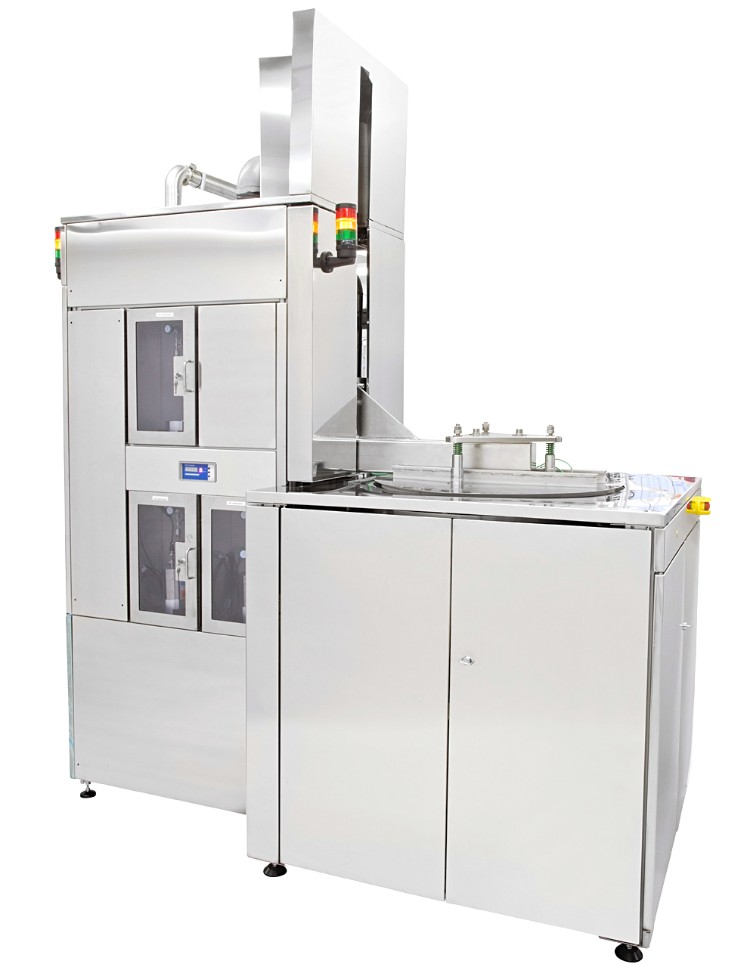
- Impressive System Capacity
- Advanced Evaporation Source
- Versatile Wafer Handling
- Automatic Load-Lock for Efficiency
- Wide Range of Applications
Email: info@sistemtechnology.com Call: +44 (0)1327 362 844
Thin Film Deposition
Equipment used to create thin films is essential in the semiconductor industry, as these films serve as the foundation for a variety of electronic devices, such as integrated circuits, solar cells, and displays. Thin film deposition equipment is designed to deposit materials with precision and uniformity on substrates, enabling manufacturers to produce high-quality components that power modern technology.
There are several thin film deposition techniques, each with its own specialised equipment. Some of the most widely used methods include:
Physical Vapour Deposition (PVD): PVD equipment, such as sputtering and evaporation systems, utilizes physical processes to deposit thin films by condensing vaporized materials onto the substrate.
Chemical Vapour Deposition (CVD): CVD equipment deposits thin films through chemical reactions involving gas-phase precursors. Common CVD techniques include plasma-enhanced CVD (PECVD), low-pressure CVD (LPCVD), and atomic layer deposition (ALD).
Electrochemical Deposition: This technique uses electrochemical processes to deposit thin films, often employed in the fabrication of semiconductor devices and MEMS.
Atomic Layer Deposition (ALD): ALD equipment enables highly precise and conformal deposition by using alternating self-limiting chemical reactions to build layers one atom at a time.
Each deposition technique offers unique advantages in terms of film quality, conformality, and process control, making them suitable for various applications within the semiconductor industry. By employing advanced thin film deposition equipment, manufacturers can continue to innovate and drive the development of increasingly powerful electronic devices.
Thin Film Deposition Products
-
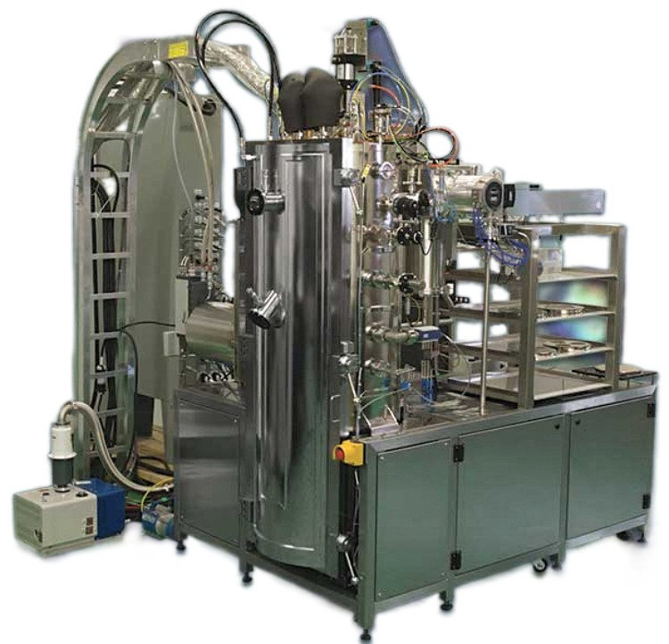
Icarus Indium Deposition System
-
Aegis Diamond-Like Carbon Deposition
- Unleash the Power of DLC
- Unrivalled Precision and Control
- Efficiency Redefined
- Reliability at Its Core
- Innovation in Design
-
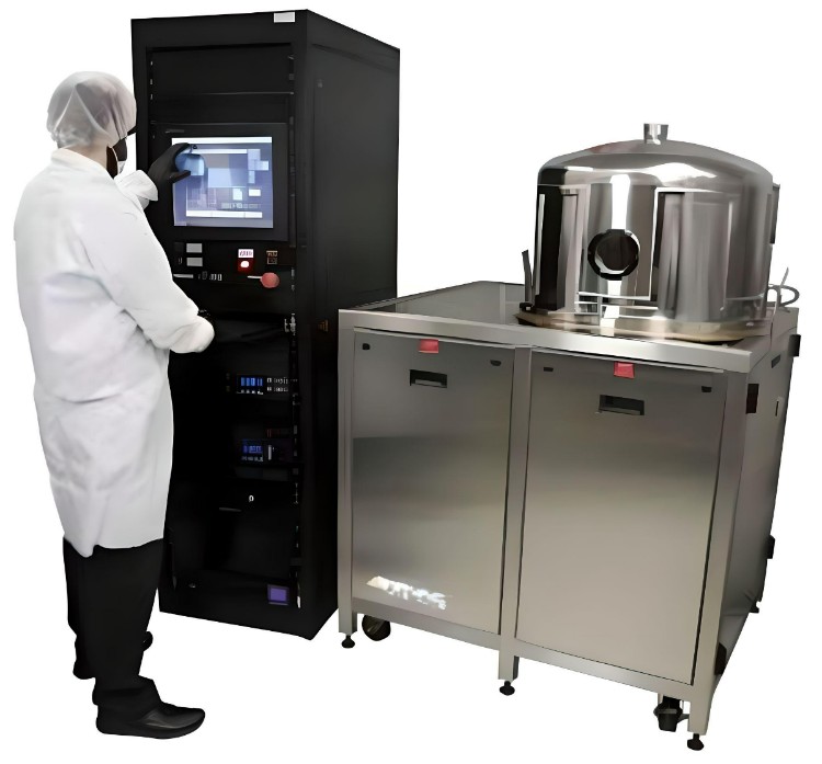
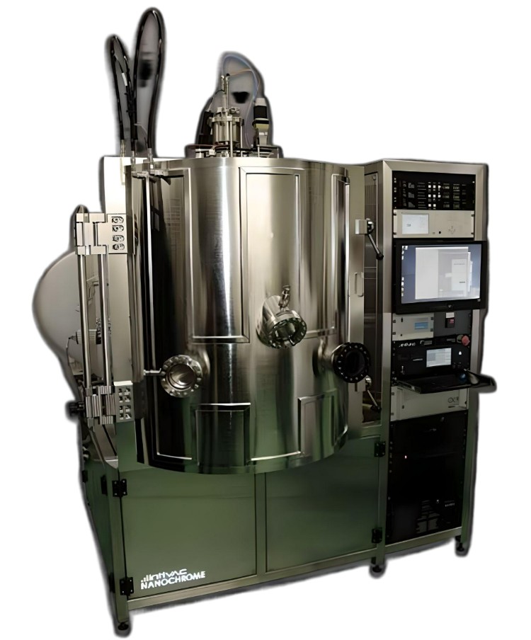
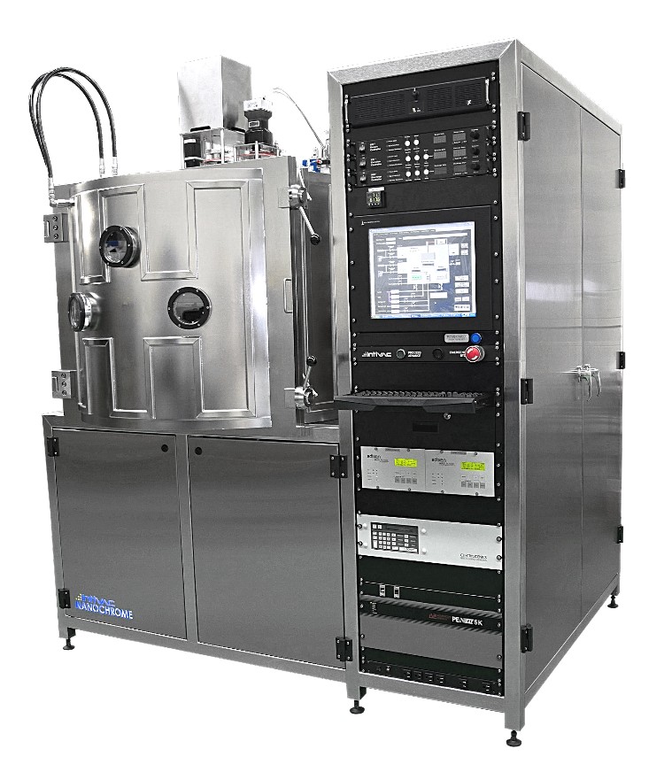
Nanochrome Pico Thin Film Deposition
- Flexible Configuration for Diverse Applications
- Compact Design with Easy Reconfiguration
- Load-Lock Transfer Capability
-
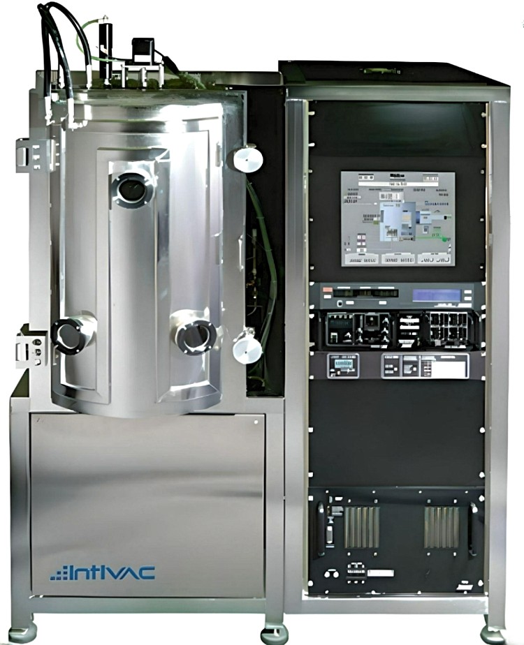
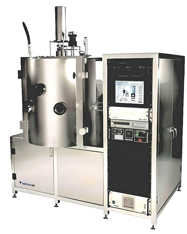
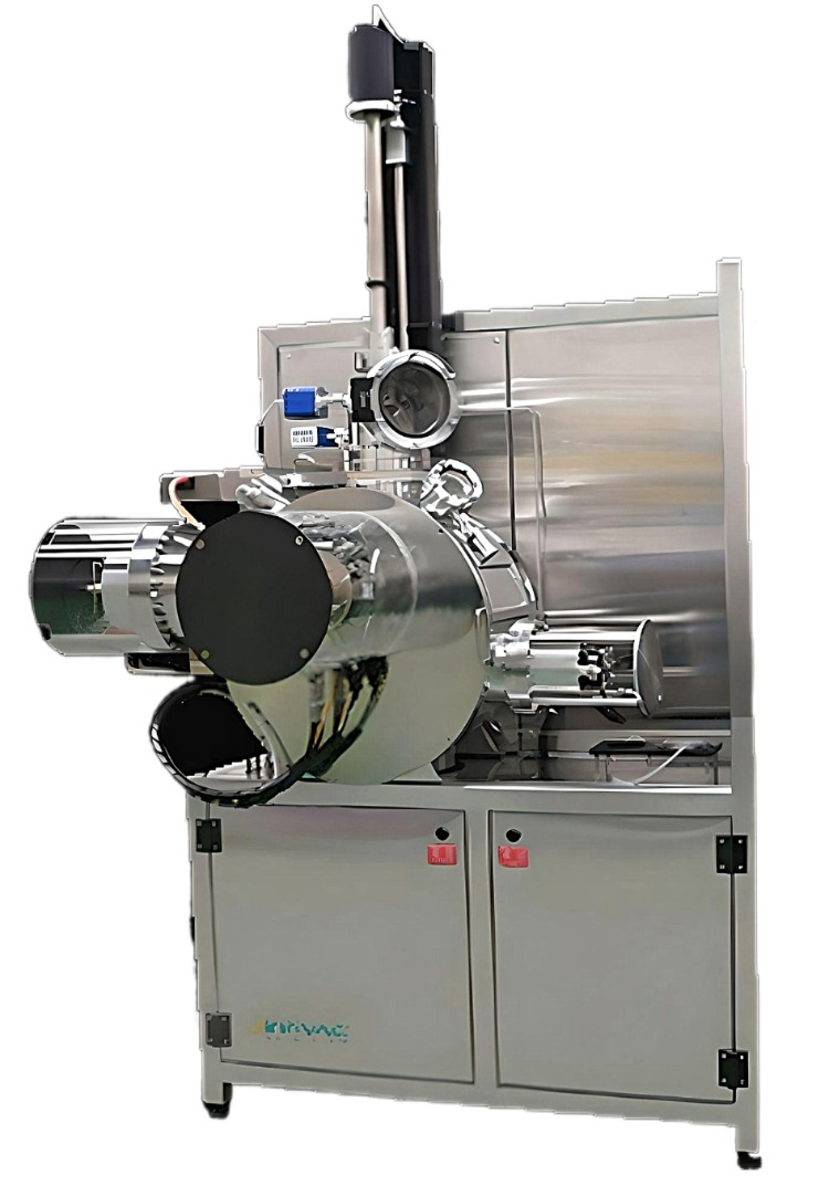
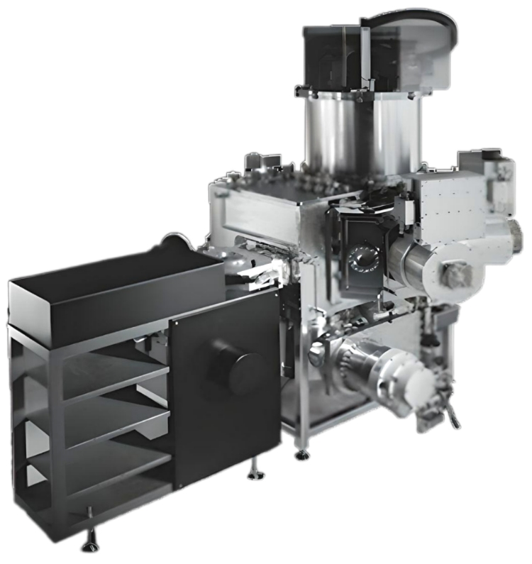
Nanochrome I Thin Film Deposition
- Multi-Layer Deposition and More
- Advanced Electron Beam Evaporation
- Direct Water-Cooled Rotating Substrate Stage
- Automatic Variable Angle Deposition
- Unlock Versatile Thin Film Deposition
-
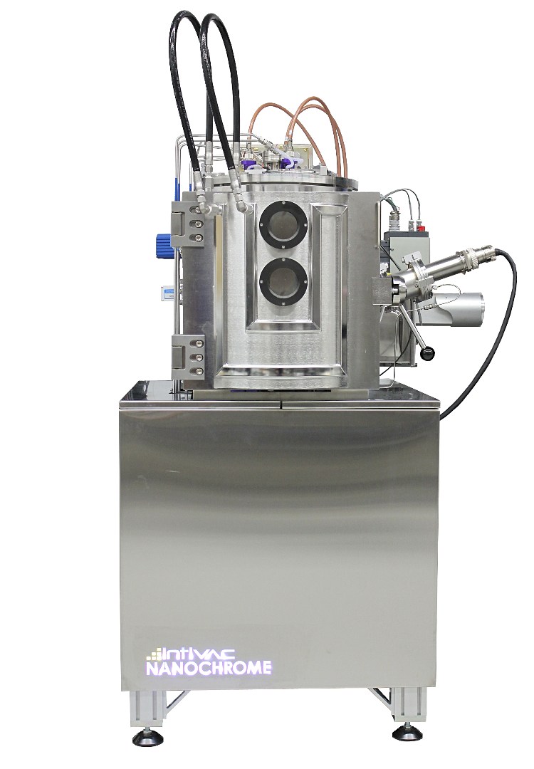
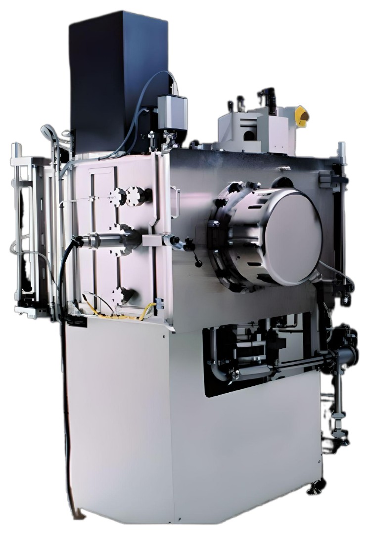
Nanochrome II Thin Film Deposition
- Explore a Wealth of Deposition Options
- Clamshell Design for Enhanced Access
- Advanced Ion Sources for Enhanced Coating
- Tailored Fixturing for Uniform Coatings
- High Vacuum Efficiency
- High-Quality Construction for Optimal Performance
- Versatile Feedthrough Ports and Optical Window
-
Nanochrome IV UV VIS Thin Film Deposition
- Dual-Axis Rotation for Enhanced Uniformity
- Real-Time Optical Monitoring
- Operator-Friendly Design
- Cutting-Edge Cryopump Technology
- Exceptional Process Repeatability With A Baseline Uniformity Of 2%
-
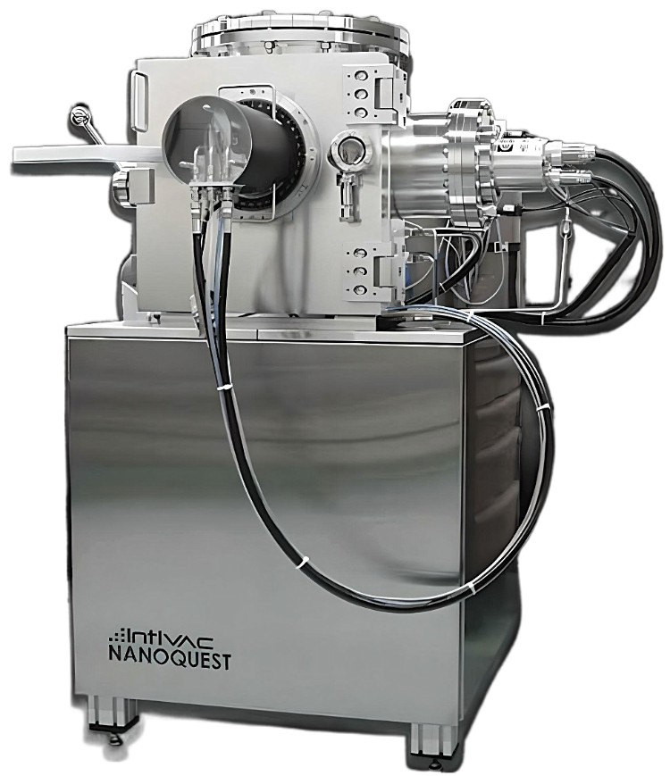
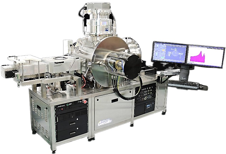
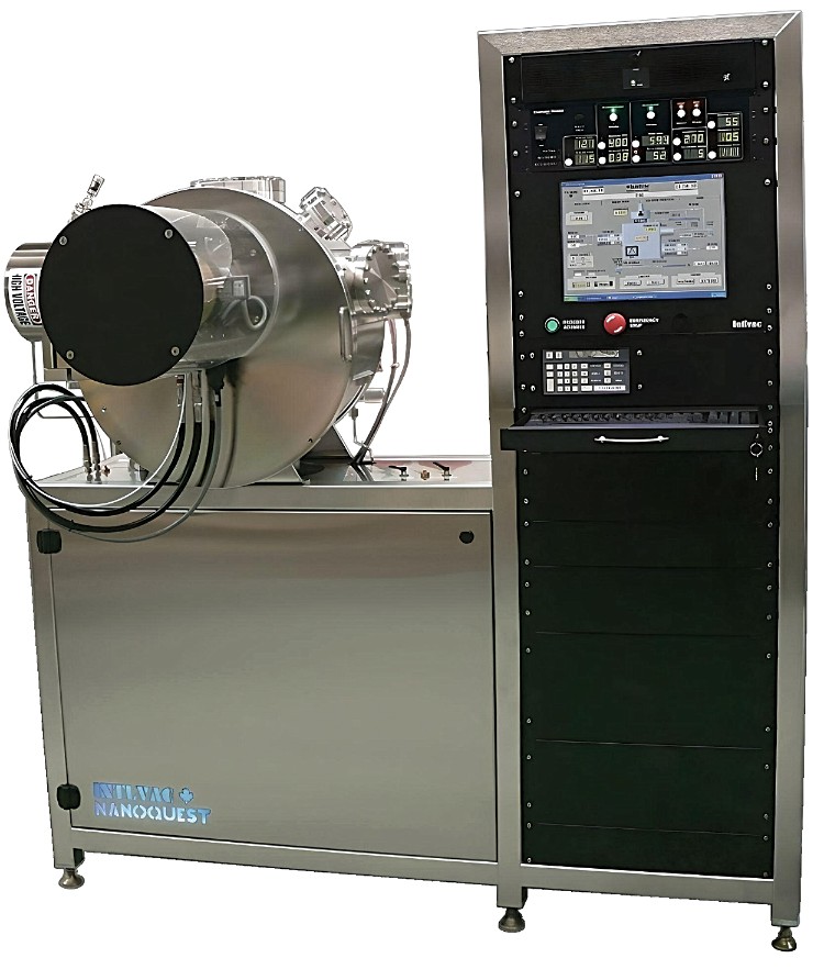
Nanoquest Pico Ion Beam Etch & Milling
- Precision Ion Beam Etching
- Fast Pumping and Ultimate Pressure
- Flexible Substrate Fixturing
- Wide Substrate Size Compatibility
- Comprehensive Ion Milling Capabilities
- Expansion Options
-
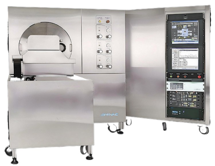
Nanoquest I Ion Beam Etch & Milling
- Compact Design, Uncompromised Performance
- Automated Excellence
- Enhanced Efficiency with Nanoquest I-LL (Load Lock) System
- Versatile Chamber Design
- Flexible Configurations for Maximum Potential
- Experience the Power of Precision
-
Nanoquest II Ion Beam Etch & Milling
- Advanced Nanofabrication Capabilities
- Flexible Configuration Options
- High-Performance Wafer Handling
- Atomic Layer Etching Capabilities
-
Nanoquest III/IV Ion Beam Etch & Milling
- Efficient Batch Processing
- Advanced Water-Cooled Double Axis Stage
- Wide Process Range
- RF Ion Source and Endpoint Detection
- Intuitive Operation and Display
- Experience Precision and Versatility
-
Nanoquest I Combo Ion Beam Sputter Deposition & Etch
- Superior PVD Deposition Capability
- Multi-Target Carousel and Water-Cooled Stage
- Full Ion Beam Etch Capability
- Compact Design with Reputable Coatings
-
Nanoquest I Ion Beam Sputter Deposition
- Versatile Deposition Capabilities
- Multi-Target Carousel
- Precision Substrate Handling
- Empowering Ion Assist Capability
- Compact Design, Premium Results
-
Nanoquest II Ion Beam Sputter Deposition
Superior PVD Deposition Capability
Large Multi-Target Carousel
Rotating and Angle-Tilt Substrate Stage
Ion Assist Capability and Monitoring
High-Density Coatings with Low Particle Levels
-
Nanoquest III Ion Beam Sputter Deposition
- Superior PVD Deposition Capability
- Efficient Batch Processing
- Multi-Target Carousel and Planetary Double Rotation
- Angle-Tilt Substrate Stage and Ion Assist Capability
- High-Density Coatings with Low Particles
-
Nanochrome IV Ion Beam Sputter Deposition
- Superior Sputter Up Geometry
- Configurable for Various Loading Options
- Multi-Target Carousel and High-Speed Substrate Stage
- Ion Assist Capability and QCM Instrumentation
- Dynamic Optical Control for Optical Applications
-
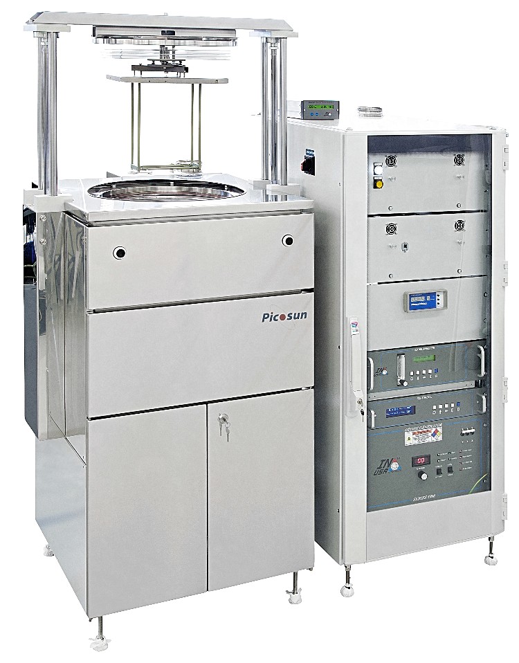
P-1000
- All kinds of 3-dimensional items such as mechanical machinery parts, glass or metal sheets, coins, watch parts and jewelry, lenses, optics, and medical equipment, surgical implants and implantable devices (PicoMEDICAL™ solutions)
- Typical processes: Al2O3, ZnO, TiO2
- Precursors: Liquid, solid, gas, ozone
- Up to 10 sources with 6 separate inlets
- Level sensors, cleaning and refill service
-
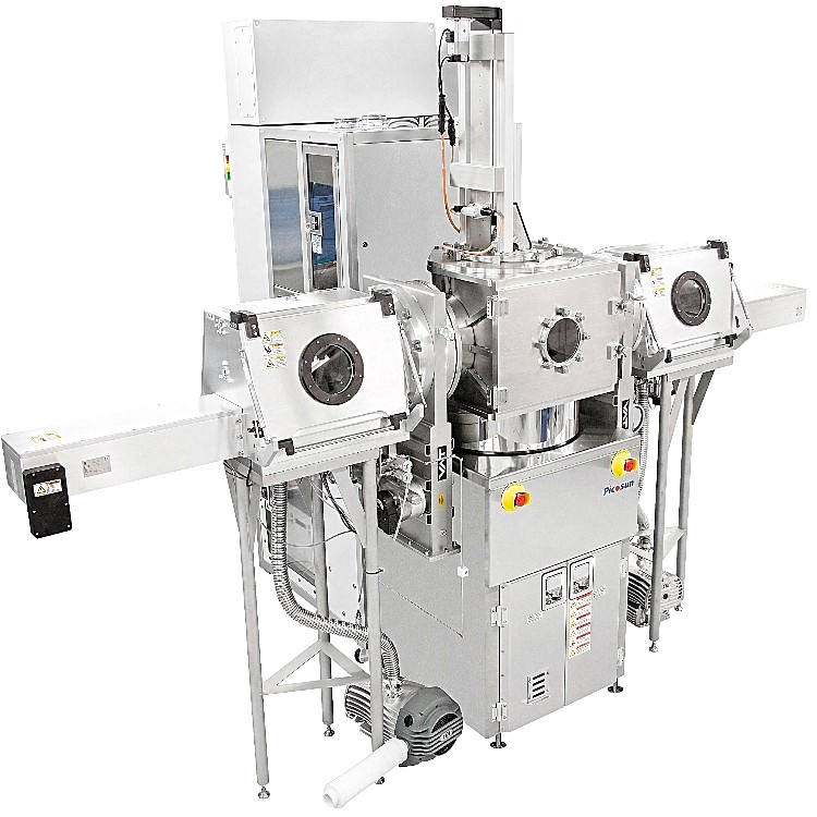
P-300B
- 200 mm wafers in batches of 25 pcs (standard pitch)
- 150 mm wafers in batches of 50 pcs (standard pitch)
- 100 mm wafers in batches of 75 pcs (standard pitch)
- All kinds of 3-dimensional items such as mechanical machinery parts, coins, watch parts and jewellery, lenses, optics, and medical equipment, surgical implants and implantable devices (PicoMEDICAL® solutions)
- High aspect ratio samples (up to 1:2500)
- 50 – 500°C
-
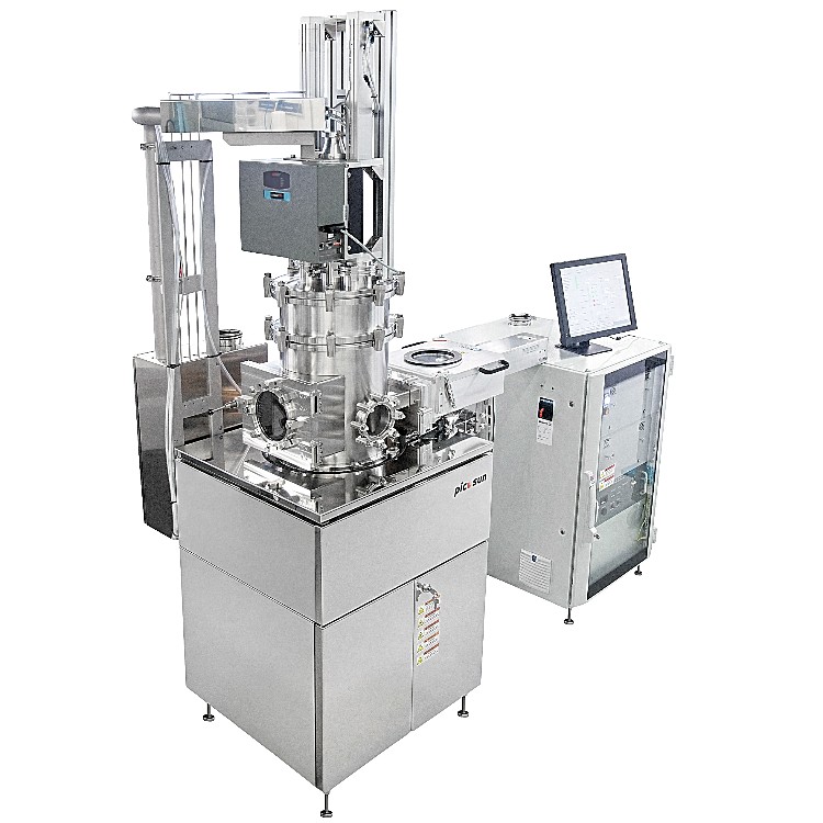
P-300BV
- Batch processes available with cycle times down to single digit seconds
- Al2O3, SiO2, Ta2O5, HfO2, ZnO, TiO2, ZrO2, AlN, TiN, and metals
- Down to <1% 1σ non-uniformity in a batch (Al2O3, WIW, WTW, B2B, 49 pts, 5mm EE)
- Liquid, solid, gas, ozone
- Up to 8 sources with 4 separate inlets
- Level sensors, cleaning and refill service
-
R-200 Advanced
- 50-200 mm single wafers
- 156 mm x 156 mm solar Si wafers
- 3D objects
- Powders and particles
- Mini-batch
- Porous, through-porous, and high aspect ratio (up to 1:2500)
- Typical processes: Al2O3, TiO2, SiO2, Ta2O5, HfO2, ZnO, ZrO2, AlN, TiN, metals such as Pt or Ir
-
R-200 Standard
- Precursors : Liquid, solid, gas, ozone (up to 6 sources with 4 separate inlets)
- Typical processes: Al2O3, TiO2, SiO2, Ta2O5, HfO2, ZnO, ZrO2, TiN, AlN, metals such as Pt or Ir
- 50 – 500°C
- 50-200 mm single wafers
- 156 mm x 156 mm solar Si wafers
- 3D objects
- Powders and particles
- Mini-batch