- Precision Ion Beam Etching
- Fast Pumping and Ultimate Pressure
- Flexible Substrate Fixturing
- Wide Substrate Size Compatibility
- Comprehensive Ion Milling Capabilities
- Expansion Options
Email: info@sistemtechnology.com Call: +44 (0)1327 362 844
Ion Beam Etching (IBE) & Ion Beam Milling (IBM)
Ion Beam Etching (IBE) and Ion Beam Milling (IBM) stand as pivotal techniques, offering unparalleled precision and control in the creation and modification of thin films. These processes utilise accelerated ions to meticulously sculpt surfaces at the microscopic and even atomic scales, making them indispensable in industries ranging from semiconductor manufacturing to precision optics and beyond.
SiSTEM Technology is very proud to distribute Intlvac Thin Film Ion Beam Etching and Ion Beam Milling tools throughout Europe, and these include the entry level Nanoquest Pico, Nanoquest I, 100 & 150mm Nanoquest II, and the Nanoquest III/IV.
Understanding Ion Beam Etching and Ion Beam Milling
Ion Beam Etching involves bombarding a material surface with accelerated ions, typically ions of noble gases such as argon or xenon. These ions impinge upon the surface, transferring their energy to the atoms in the material. This energy can break atomic bonds, removing material from the surface and creating the desired patterns or structures with remarkable precision. Ion beam etching is widely used for pattern transfer, surface smoothing, and creating nanoscale features that are crucial in semiconductor device fabrication and microelectronics.
Ion Beam Milling, on the other hand, focuses on the precise removal of material to achieve specific thicknesses or shapes. It is particularly effective for thinning samples to electron transparency for transmission electron microscopy (TEM) analysis or for creating ultra-thin films with uniform thicknesses. This technique is highly valued in materials science research, where the ability to precisely control film thicknesses down to the atomic level is essential.
The Benefits of Ion Beam Etching and Milling
Sub-Micron Precision
Ion beams offer exquisite control over feature sizes and depths, achieving sub-micron resolutions that are crucial for manufacturing cutting-edge electronic devices and optical components. This level of precision ensures reliability and performance in high-tech applications where tolerances are incredibly tight.
Damage-Free Processing
Unlike some traditional etching methods that can introduce damage to the material, ion beam techniques operate in a low-temperature environment and with minimal physical contact. This results in minimal structural damage to the substrate, preserving the integrity of delicate materials and enabling the fabrication of defect-free surfaces.
Versatility Across Materials
Ion beam etching and milling are compatible with a wide range of materials, from semiconductors like silicon and gallium arsenide to metals, ceramics, and polymers. This versatility makes these techniques adaptable to various industries, including aerospace, medical devices, and telecommunications, where diverse material properties are encountered.
Uniformity and Reproducibility
Consistency is critical in manufacturing and research & development. Ion beam processes excel in delivering uniformity across large areas and ensuring reproducibility from batch to batch. This reliability enhances the yield and quality of fabricated components, reducing variability and increasing productivity.
Tailored Surface Modification
Beyond mere material removal, ion beams can be used to modify surface properties such as roughness, wettability, and optical reflectivity. This capability is invaluable in designing surfaces with specific functionalities, such as anti-reflective coatings or hydrophobic layers, to meet exacting performance requirements.
Integration with Nanotechnology
As nanotechnology continues to advance, ion beam techniques play a pivotal role in enabling the fabrication of nanostructures and nanoscale devices. The ability to precisely sculpt materials at the atomic level is fundamental to realising the potential of nanotechnology in fields such as quantum computing, nano-electromechanical systems (NEMS), and advanced sensors.
Applications in Industry and Research & Development
The applications of ion beam etching and milling are diverse and expanding. In semiconductor manufacturing, these techniques are used for defining circuit patterns and improving device performance. In optics, they enable the creation of precise optical elements with tailored surface characteristics. In materials science, researchers leverage ion beams to study the properties of thin films and nanostructures, pushing the boundaries of what is possible in materials design and characterisation.
Ion beam etching and ion beam milling represent a cornerstone of modern materials fabrication, offering unparalleled precision, versatility, and control. As industries demand increasingly sophisticated devices and materials, these techniques continue to evolve, driving innovation across disciplines and enabling the development of next-generation technologies. Whether in the clean rooms of semiconductor fabs or the laboratories of materials scientists, ion beam processing remains essential for achieving the highest standards of quality and performance in thin film fabrication.
Embracing the capabilities of ion beam etching and milling is not just about meeting current challenges; it is about unlocking new possibilities for the future of technology and scientific discovery. As research & development and industry converge on the frontier of nanoscale engineering, these techniques will undoubtedly play a central role in shaping our technological landscape for years to come.
Contact us today to find out how we can assist your project with our expertise.
Get a quote quickly by clicking the link and submitting your requirements via our quote request page.
Ion Beam Etching (IBE) and Ion Beam Milling (IBM) Tools
-
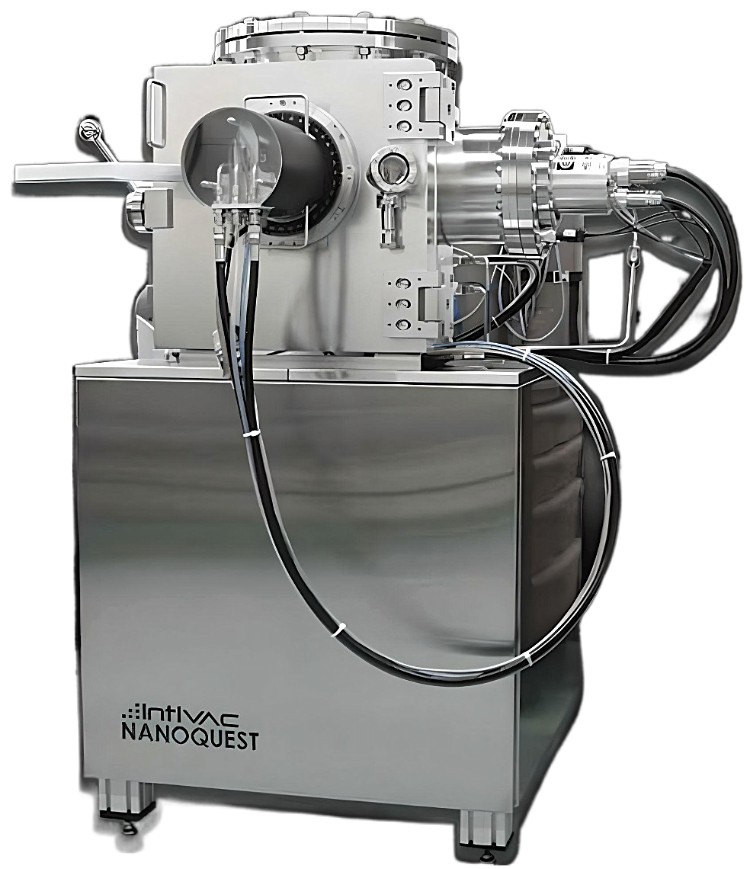
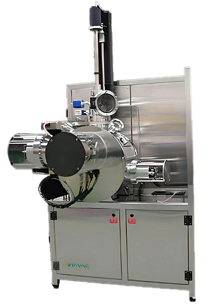
Nanoquest Pico Ion Beam Etch & Milling
-
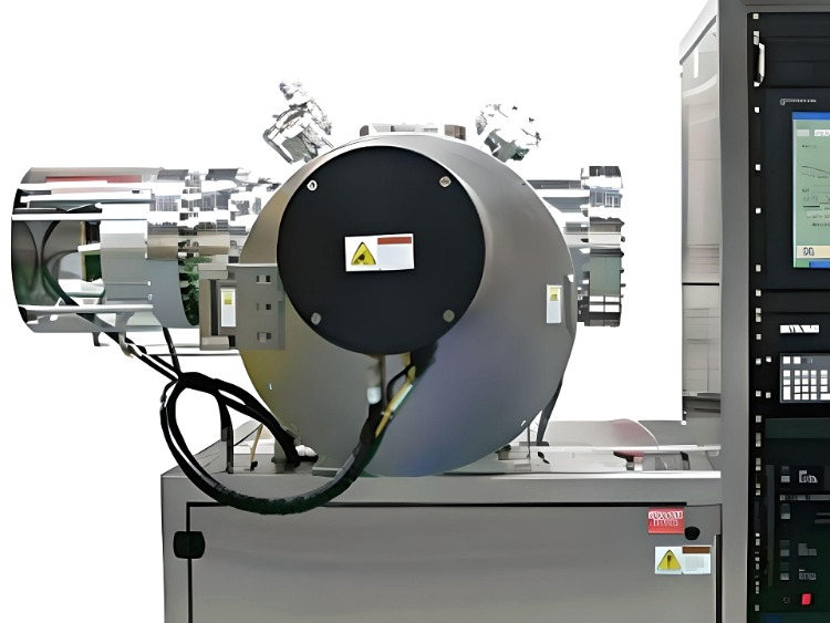
Nanoquest I Ion Beam Etch & Milling
- Compact Design, Uncompromised Performance
- Automated Excellence
- Enhanced Efficiency with Nanoquest I-LL (Load Lock) System
- Versatile Chamber Design
- Flexible Configurations for Maximum Potential
- Experience the Power of Precision
-
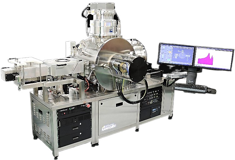
Nanoquest II Ion Beam Etch & Milling
- Advanced Nanofabrication Capabilities
- Flexible Configuration Options
- High-Performance Wafer Handling
- Atomic Layer Etching Capabilities
-
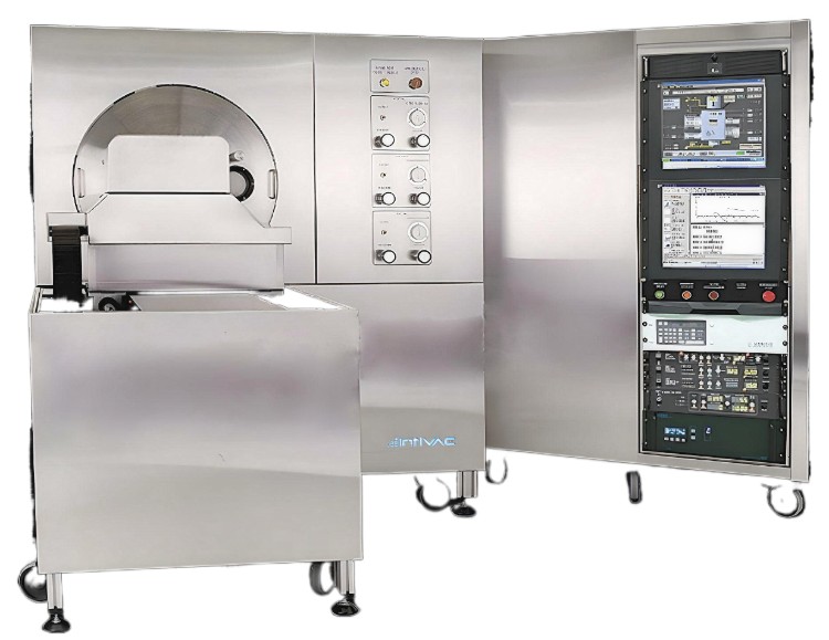
Nanoquest III/IV Ion Beam Etch & Milling
- Efficient Batch Processing
- Advanced Water-Cooled Double Axis Stage
- Wide Process Range
- RF Ion Source and Endpoint Detection
- Intuitive Operation and Display
- Experience Precision and Versatility
-
Nanoquest I Combo Ion Beam Sputter Deposition & Etch
- Superior PVD Deposition Capability
- Multi-Target Carousel and Water-Cooled Stage
- Full Ion Beam Etch Capability
- Compact Design with Reputable Coatings