- Versatile Substrate Compatibility
- Advanced Thermal Management
- Void-Free Bonding Process
- High Throughput with Exceptional Yield
- Outstanding System Uptime & Serviceability
- Comprehensive Process Monitoring
Email: info@sistemtechnology.com Call: +44 (0)1327 362 844
Temporary Wafer Bond & Debond Tools
In the quest for more compact and powerful semiconductor devices, wafer bonding technology plays a pivotal role in wafer processing. The Cost Effective Equipment Apogee Temporary Wafer Bonding and Wafer Debonding tools offer sophisticated solutions, enabling the coating of full-thickness wafers with adhesive, securely bonding them to support carriers, and facilitating their thinning for intricate downstream processes. This addresses critical factors like flatness, alignment precision, void elimination, temperature consistency, coefficient of thermal expansion (CTE) compatibility, and bonding force to ensure high-quality, reliable semiconductor devices.
Temporary wafer bonding is vital for the production of 3D integrated circuits (ICs), power devices, and Fan-Out Wafer Level Packaging (FoWLP) wafers, as well as in managing delicate substrates such as compound semiconductors.
The Essence of Wafer Bonding
With the semiconductor industry’s shift towards smaller, yet more powerful devices, the demand for advanced wafer bonding solutions has surged. Temporary substrate bonding, especially for substrates thinner than 100µm, presents unique challenges. The Cost Effective Equipment Temporary Wafer Bonding and Debonding tools efficiently mitigate these by minimising breakage risks and enabling precise downstream processing such as through-silicon vias (TSV) and metal-plating. Following these processes, the bonded pair is debonded, cleaned, diced, and packaged, ready for integration.
Optimised Bonding Conditions
Following the adhesive material specifications, the Cost Effective Equipment Apogee Temporary Wafer Bonding system’s platens are heated to the ideal temperature, ensuring the adhesive reaches its optimal state for maximum adhesion. The device wafer, precisely aligned and centred on the lower platen, is bonded to the carrier wafer, with mechanical fixtures maintaining alignment without direct contact at loading.
Vacuum-Sealed Bonding Chamber
Once aligned, the bonding chamber is sealed, and vacuum applied to remove air, with programmable piston force ensuring uniform adhesive spread and full wafer coverage. After bonding, the wafer pair is cooled on a dedicated plate, solidifying the adhesive for robust bond strength, preparing it for subsequent processing.
Critical Parameters for Superior Quality
The quality of wafer bonding is influenced by several crucial factors, now more significant than ever due to the industry’s evolution towards finer features and thinner substrates.
Flatness (TTV): Ensures uniform bonding, eliminating voids that could weaken the structural integrity of the device.
Alignment: Critical for uniform bonding and high device yield, impacting downstream processing accuracy.
Voids: Their elimination is vital for the uniformity of bonded layers, preventing potential breakage or delamination.
Temperature Control: Guarantees uniform adhesive flow, essential for consistent bonding and material integrity.
CTE Compatibility: Reduces stress during temperature changes, preventing delamination and ensuring the durability of the bond.
Bonding Force: The right force ensures a strong, uniform bond, crucial for the device’s performance and reliability.
Designed for the high demands of semiconductor production, the Apogee Temporary Wafer Bonding tool is a comprehensive solution for temporary adhesive wafer bonding, supporting a vast array of debonding materials. It prioritises high yield and throughput without necessitating full automation, making it an ideal choice for various wafer sizes and a weekly volume of 400-1,000 wafers.
Intuitive Control and Precision
The Apogee Temporary Wafer Bonding tool’s control panel offers a user-friendly interface for real-time updates, process parameter adjustments, and comprehensive monitoring, ensuring a seamless bonding process. Its mechanical alignment fixtures and dual ultra-flat, self-levelling heated platens provide unmatched precision, with temperature uniformity and bonding TTV optimized for each operation.
Customised to Your Needs
Whether accommodating nonstandard wafers and carriers or adjusting for precise bonding conditions, the Cost Effective Equipment Apogee Temporary Wafer Bonder is adaptable to your specific requirements, ensuring the integrity and reliability of your semiconductor devices.
Wafer Debonding
Once these essential steps are completed, the bonded wafer assembly is then carefully debonded for further processing or integration into final products. Debonding products and processes, on the other hand, are designed to gently release the carrier from the wafer or substrate after processing is complete. This step may involve the use of the Cost Effective Equipment 1300CSX Thermal Slide Debonder or the Cost Effective Equipment Apogee Mechanical Wafer Debonder, or chemical methods, depending on the bonding material used and the specific requirements of the process. Once the device wafer is debonded from the carrier wafer it can be used either sent for further processing or integration into final products.
Why Temporary Wafer Bonding and Debonding?
Enabling Thinner Wafers
As devices shrink and functionality increases, the need for thinner wafers becomes paramount. Temporary bonding tools allow wafers to be thinned beyond what was previously possible, supporting the advancement of ultra-thin and flexible electronics.
Complex Device Fabrication
Advanced semiconductor devices, including 3D stacked integrated circuits (ICs) and microelectromechanical systems (MEMS), require multiple layers of fabrication. Temporary bonding and debonding tools provide the means to handle and process these layers individually before final assembly, ensuring the integrity and performance of the final device.
Enhanced Process Flexibility
Temporary bonding and debonding technologies offer unmatched process flexibility, accommodating a wide range of materials and processing conditions. This adaptability is crucial in a field where innovation and material diversity are constant.
Benefits of Temporary Bonding and Debonding Tools
Increased Yield and Reliability
By enabling the handling of wafers and devices through various processing steps without damage, these tools significantly increase the yield and reliability of semiconductor products. The precision with which wafers can be bonded, processed, and then debonded minimizes defects and improves the overall quality of the semiconductor devices.
Cost Efficiency
The ability to process thinner wafers and more complex devices without loss or damage reduces material costs and increases the efficiency of the fabrication process. This cost efficiency is vital in maintaining competitive advantage in the semiconductor industry.
Innovation Support
Temporary bonding and debonding technologies are pivotal in the development of next-generation semiconductor devices. By facilitating the processing of new materials and complex structures, these tools support the continuous innovation that drives the industry forward.
Industries and Applications
Semiconductor Manufacturing
At the heart of the semiconductor manufacturing industry, temporary bonding and debonding tools are used in the fabrication of standard and advanced ICs, supporting processes such as wafer backgrinding, etching, and layer stacking.
MEMS and Sensors
In the production of MEMS and sensors, these tools enable the precise handling and processing of delicate structures, ensuring the functionality and reliability of these critical components in automotive, medical, and consumer electronics.
Advanced Packaging
Temporary bonding and debonding play a key role in advanced packaging techniques, such as 3D IC integration and wafer-level packaging, where multiple semiconductor devices are integrated into a single package for enhanced performance and functionality.
Flexible and Wearable Electronics
The flexibility afforded by temporary bonding and debonding technologies is essential in the burgeoning field of flexible and wearable electronics, enabling the creation of devices that are not only powerful but also lightweight and bendable.
The Cost Effective Equipment Temporary Wafer Bonding and Debonding tools stand at the forefront of semiconductor fabrication technology, offering unmatched precision, flexibility, and efficiency. As the industry continues to push the boundaries of device miniaturisation and complexity, the Apogee Temporary Wafer Bonding and Debonding tools provide the solutions needed to meet these challenges head-on, driving the future of semiconductor wafer processing and innovation.
Contact us if you have any questions before requesting a quote to discover how this state-of-the-art equipment can revolutionise your wafer processing and help you achieve exceptional results.
Get a quote today for the Cost Effective Equipment Temporary Wafer Bonding and Debonding tools.
Temporary Bond & Debond Products
-
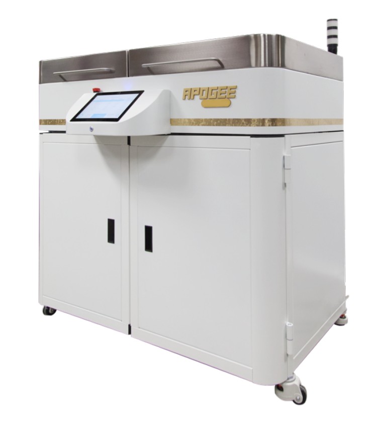
Apogee Temporary Wafer Bonder
-
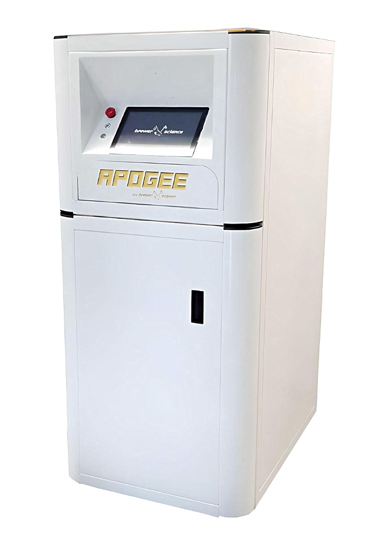
Mechanical Wafer Debonder
- Minimised Stress
- High Throughput
- Room Temperature Operation
- Secure Wafer Handling
- Clean and Efficient
- Precision Force Application
-
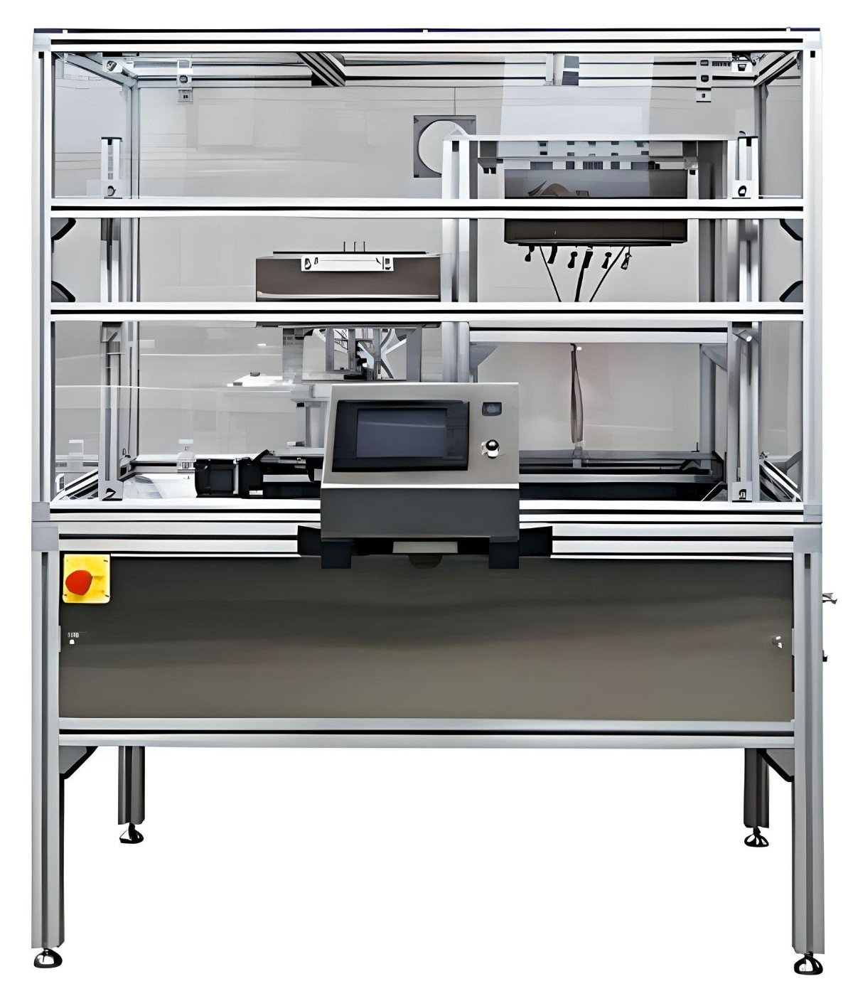
1300CSX Thermal Slide Debonder
- SiC, GaN, GaAs, InP, Sapphire, Silicon, and Glass
- 2-inch, 3-inch, 100 mm, 125 mm, 150 mm, and 200 mm wafers
- Maximum Platen Temperature up to 300°C
- Bond line axis with a precision of ±1.5 nm
- Throughput: 8-14 WPH for wafers <200 mm and 4-8 WPH for wafers >200 mm