Email: info@sistemtechnology.com Call: +44 (0)1327 362 844
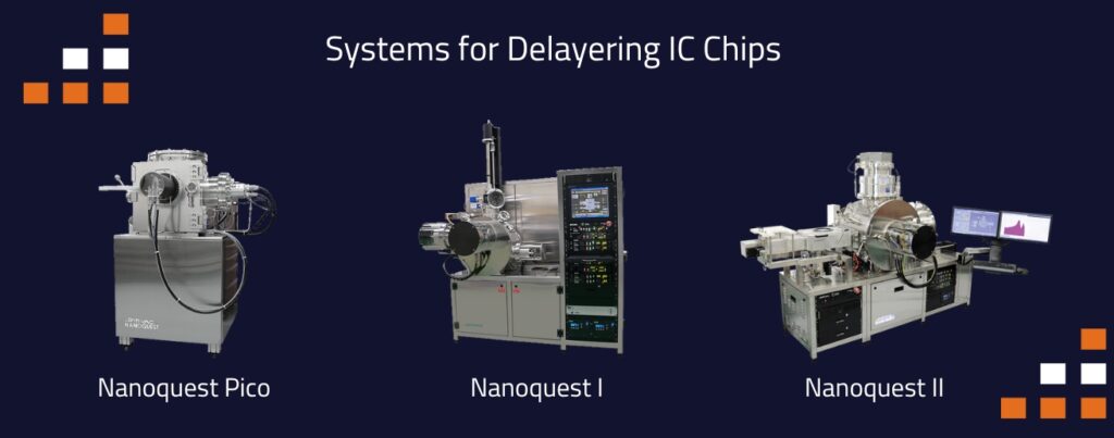
Delayering Systems by Intlvac: Revolutionising Failure Analysis in the Semiconductor Industry
In the semiconductor industry, the ability to meticulously deconstruct or “delayer” wafer-level integrated circuits (ICs) is paramount. This process, crucial for failure analysis and reverse engineering, allows engineers to examine the intricate internal structures of IC devices. Intlvac, a leader in advanced material processing technologies, offers state-of-the-art delayering systems designed to meet the demanding requirements of modern semiconductor analysis.
Understanding Delayering in Semiconductor Analysis
Integrated circuits, or ICs, are minuscule chips, typically ranging from 4mm x 4mm to 25mm x 25mm in size. These chips are constructed on a silicon substrate, layered with micrometer-thin to nanometer-thin films of various electronic materials. These layers form a complex network of conductive metals, insulating dielectrics, and semiconductor materials, usually stacked in 5 to 12 layers. A simple passive layer might include aluminium or copper lines encased in a thin barrier layer made of tantalum or titanium-based materials, all embedded in a silicon-based dielectric matrix.
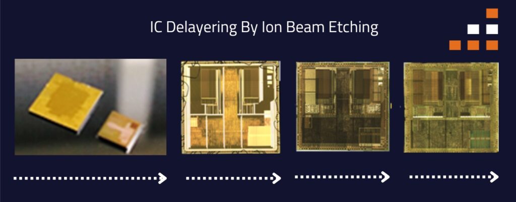
The demand for precise analysis of these IC structures necessitates a meticulous delayering process, which involves sequentially removing each layer to expose the layers beneath. Traditional delayering techniques, however, are increasingly inadequate for contemporary IC designs, which feature thinner layers and more compact structures. This evolution in IC design calls for advanced delayering methods capable of removing nanometer-thick materials uniformly across the entire chip.
The Challenges of Delayering
The primary objective of delayering is to remove material in a way that reveals a common plane of the IC chip without penetrating adjacent layers. A failed delayering step can expose unintended materials and structures, complicating the analysis. Effective delayering techniques must create a smooth, uniform planar surface while precisely controlling the removal of micrometer, nanometer, and atomic levels of material. The challenge is further compounded by the need to deal with multiple materials, each with unique properties affecting their removal characteristics.
Intlvac’s Ion Beam Etching (IBE) Technology
Intlvac’s ion beam etching (IBE) technology stands out as a superior solution for delayering modern IC chips. Here’s why:
- Universal Etchant Process: IBE can remove any material through a purely physical sputtering process. This makes it ideal for etching metals, alloys, insulators, semiconductors, carbon-based materials, and multilayer composites. The ability to control ion beam properties, such as ion energy, ion current density, and incidence angle, allows for precise control over the etching process.
- Material Etch Selectivity: By selecting appropriate feed gases, IBE can optimize etch rates to preferentially remove specific materials. This ensures uniform removal of different materials within an IC layer, producing the desired planar surfaces.
- Precision and Control: IBE excels at removing material at atomic levels, allowing for nanometer-scale resolution in delayering. This precision ensures that the process stops at the desired layer, avoiding the risks of undershoot or overshoot common in traditional methods.
- Planarization: IBE can smooth surfaces by controlling the incidence angle of the ion beam, enhancing the removal of elevated structures over the base layer. This capability eliminates the need for mechanical polishing slurries and polishes surfaces on an atomic/molecular scale.
- Uniform Material Removal: The broad ion beam used in IBE is significantly larger than IC chips, ensuring uniform material removal with less than 1% non-uniformity. This uniformity is crucial for forming and maintaining common layers deep within the IC structure.
- Minimised Side Effects: Unlike mechanical polishing, wet chemical etching, or dry plasma etching, IBE minimizes residual contamination, damage, and exposure to heat and radiation. This ensures the integrity of subsequent measurements and analysis, preserving the native state of the IC materials.
Why Choose Intlvac?
Intlvac’s delayering systems, powered by advanced IBE technology, provide a robust and precise solution for the semiconductor industry’s evolving needs. As IC designs become more complex and densely packed, the demand for accurate and efficient delayering techniques grows. Intlvac’s commitment to innovation ensures that their systems meet these challenges, offering unparalleled precision and reliability for failure analysis and reverse engineering of IC devices.
By leveraging Intlvac’s expertise and cutting-edge technology, semiconductor professionals can achieve superior results in their delayering processes, paving the way for continued advancements in microelectronics and semiconductor design.